1D Devices for Ge and 2D Materials Utilizing 3D Integration Technology

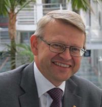
Speaker: Mikael Östling
Affiliation: KTH Royal Institute of Technology
Abstract: Digital electronics is constrained by time delay as well as power and energy consumption. In a die, electrical energy is converted into heat at standby (static leakage current in MOSFET), during computation (switching of MOSFET devices) and upon data transport (switching of metal interconnects). Currently as much as 50 % of the dynamic power is consumed by switching the interconnects in a modern microprocessor. Since the on-die global metal wire length does not scale (due to RC-delay constrains), the preservation of today’s IC architecture will cause an absolute predominance of interconnects on the overall power consumption, and make the systems totally energy inefficient. On the other hand, more and more researchers believe that device scaling will finally slow down. The challenge in the future is to increase the device density without scaling the device itself and develop more energy efficient ICs which are free from severe interconnect power consumption.
In this talk, we will discuss the advantage of 3D integration to increase the device density without scaling the devices, and shorten the interconnect length to reduce the power consumption. These 3D integrated transistors are of nanowire dimension and hence can be referred as one-dimensional. Moreover, we will discuss novel photonic interconnects based on Ge and 2D layered materials (such as graphene and MoS2) to essentially provide low power consumption and high bandwidth.
Biography: Mikael Östling received his MSc and the PhD degrees from Uppsala University, Sweden. He holds a position as professor in solid state electronics at KTH, Royal Institute of Technology in Stockholm, Sweden. He is deputy president of KTH and currently department head of electronics. He was the dean of the School of Information and Communication Technology, KTH, between 2004–12. Östling was a senior visiting Fulbright Scholar at Stanford University, and a visiting professor with the University of Florida, Gainesville. In 2005 he co-founded the company TranSiC, acquired in full by Fairchild Semiconductor 2011. He was awarded the first ERC grant for advanced investigators. His research interests are nanoscaled Si and Ge device technologies and emerging 2D materials, as well as device technology for wide bandgap semiconductors for high power / high temperature applications. He has supervised 37 PhD theses work and co -authored 500+ scientific papers published in international journals and conferences. Mikael Östling was an editor of the IEEE Electron Device Letters 2005-2014 and appointed vice president of EDS 2014-15. He is editor in chief of the IEEE J-EDS since 2016. Mikael is a Fellow of the IEEE.
For more information, contact Prof. Subramanian Iyer (s.s.iyer@ucla.edu)
Date/Time:
Date(s) - Jun 05, 2017
3:00 pm - 4:00 pm
Location:
EE-IV Shannon Room #54-134
420 Westwood Plaza - 5th Flr., Los Angeles CA 90095
