‘Junction-Level’ Heterogeneous Integration of III-V Materials with Si CMOS for Novel Asymmetric Field-Effect Transistors

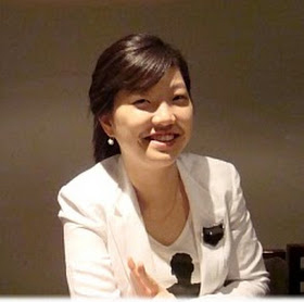
Speaker: Yoon Jung Chang
Affiliation: Ph.D. Candidate - UCLA
Abstract: Driven by Moore’s law, semiconductor chips have become faster, denser and cheaper through aggressive dimension scaling. The continued scaling not only led to dramatic performance improvements in digital logic applications but also in mixed-mode and/or communication applications. Moreover, size/weight/power (SWAP) restrictions on all high-performance system components have resulted in multi-functional integration of multiple integrated circuits (ICs)/dies in 3D packages/ICs by various system-level approaches such as System-in-Package (SiP) and through-silicon via (TSV). However, these approaches still possess shortcomings due to interconnect and power density issues as well as limited level of integration. In order to truly benefit from the most advanced digital technologies, the future high-speed/high power devices for communication applications need to be fully integrated into a single CMOS chip. Such System-on-Chip (SoC) solution can provide diverse functionalities with unprecedented levels of integration. However, Si device performance is inadequate in communication applications where very high frequency and/or power are necessary, and therefore, III-V compound semiconductors (CS) have been extensively utilized due to their superior transport and breakdown characteristics. Despite III-V CS materials performance boost, they are not cost-effective and integration density is low. In this regard, heterogeneous integration of CS materials/devices with Si CMOS platform has emerged as a viable solution to low-cost high-performance ICs. Currently, the highest performance SoC system can be achieved via integration of different technologies by integrating high-quality CS materials on Si CMOS. In this talk, we first discuss three-dimensional transistor architecture options, i.e. vertical double-gate MOSFET and planar tri-gate MOSFET. We present channel and drain engineering approaches in these field-effect transistors to integrate III-V CS materials with Si CMOS for improved device performance in mixed-mode and/or communication applications. Then, growth, characterization and electrical analysis on small-area (diameter < 100nm) complete selective-area epitaxy of GaAs/GaN will be demonstrated for achieving ‘defect-free’ III-V CS film on a Si(100) substrate. Based on a success in defect-free heterogeneous III-V film growth, we propose a novel ultra-scaled ‘junction-level’ heterogeneous integration onto mainstream Si CMOS platform. Device architecture and its key features to overcome aforementioned challenges will be given to demonstrate the potential to improve the overall device performance with diverse functionality.
Biography: Yoon Jung Chang graduated from SungKyunKwan University, South Korea, in 2008 with a Bachelor of Science degree in both Electrical Engineering and Materials Science and Engineering. Before joining Professor Jason Woo’s CMOS Research Lab at University of California, Los Angeles (UCLA), she worked in Mobile Communications at LG Electronics Inc., South Korea, as a research engineer. She received her Master of Science degree in Electrical Engineering from UCLA, in 2010. From December 2011 to March 2012, she worked as an interim engineering intern in Qualcomm CDMA Technology at Qualcomm, Inc., participating in device target simulations/analysis for high-performance 28nm/SoC 20nm technologies as well as low-power 28nm technology. She is currently a Ph.D. candidate of Electrical Engineering at UCLA, and her research interests include novel design and fabrication technologies of various nanoscale asymmetric field-effect transistor architectures for future heterogeneous integration with Si CMOS.
For more information, contact Prof. Jason C. S. Woo (woo@ee.ucla.edu)
Date/Time:
Date(s) - Sep 29, 2016
10:00 am - 12:00 pm
Location:
E-IV Tesla Room #53-125
420 Westwood Plaza - 5th Flr., Los Angeles CA 90095
