Industrial Applications of
Low Temperature Plasma Physics
Plasmas are gases
that are so hot that electrons have come off the atoms, forming a negatively
charged fluid which is mixed with the positively charged ions. The entire
plasma is electrically neutral, but its behavior is complex because the
particles' motions are controlled by electric and magnetic fields. Though
the main applications of plasma physics are to space exploration and to
controlled fusion (reproducing on earth the energy source of stars), the aspect
that affects our everyday lives is the use of plasmas in manufacturing.
For example, metals, such as propeller blades, are hardened with a plasma
surface treatment; plastics, such as automobile bumpers and potato chip bags,
are plasma treated for better paint adhesion; camera lenses have optical
coatings applied with a plasma; and synthetic diamonds can be made with a plasma
arc. The most important practical use of plasmas is, however, in the
manufacture of semiconductor circuits, particularly computer chips.
In making a
computer chip, which may contain as many as a billion transistors, the feature sizes
have to be as small as 20 nm.(nanometers). Purely chemical
etching is much too crude; plasma etching is required. In processing a
silicon wafer, perhaps half of the steps require plasma processing, and the
machines required for this account for over half the cost of the factory.
These plasma "reactors" were developed originally by trial and error
without the help of plasma physicists. In recent years there has been a
continuous improvement in the accuracy and efficiency of these reactors, and it
is becoming more clear how they work.
In UC LA's Low
Temperature Plasma Technology Laboratory (LTPTL), experimental and theoretical
work is done to understand the physical mechanisms in plasma generators so that
one can design
better ones. For instance, the helicon source, which we have been
studying for over 20 years, can produce denser plasmas with less radiofrequency (RF)
power. The reasons for its superiority, however, were mysterious, and the
understanding of this source led to many fascinating research results. One
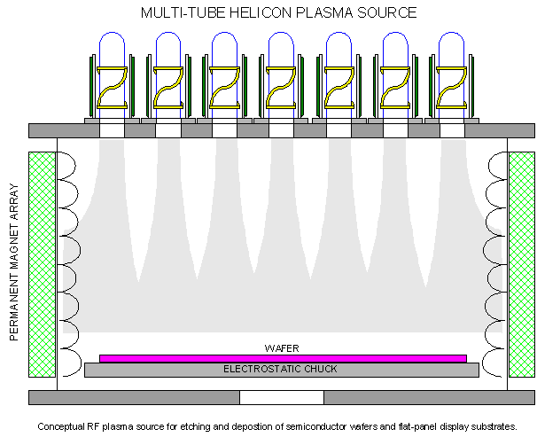
previous project was to make an array of helicon sources which can produce a wide
plasma capable of etching a large substrate uniformly, as shown by the diagram
on the left. Click on the thumbnail to expand the image, and
again on the icon at the lower right of the image for full screen. Use the
BACK button on your browser to resume.
LA's Low
Temperature Plasma Technology Laboratory (LTPTL), experimental and theoretical
work is done to understand the physical mechanisms in plasma generators so that
one can design
better ones. For instance, the helicon source, which we have been
studying for over 20 years, can produce denser plasmas with less radiofrequency (RF)
power. The reasons for its superiority, however, were mysterious, and the
understanding of this source led to many fascinating research results. One
previous project was to make an array of helicon sources which can produce a wide
plasma capable of etching a large substrate uniformly, as shown by the diagram
on the left. Click on the thumbnail to expand the image, and
again on the icon at the lower right of the image for full screen. Use the
BACK button on your browser to resume.
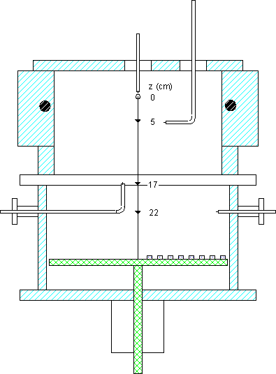
Another project
has to do with Inductively Coupled Plasmas (ICPs), which are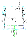 commonly
used today. These machines do not need a magnetic field, as do helicon
sources, and it is a puzzling how the RF energy gets into the center of the
plasma to produce a uniform density, when the RF field should be shielded by the
plasma. By studying these sources in a laboratory device such as shown on
the right, we have discovered that nonlinear effects can cause a number of
energetic electrons to reach the interior and produce plasma there. An
interesting problem is how an ICP turns into a helicon source as a small
magnetic field is applied. Nothing much happens until the field is large
enough to support a helicon wave. A computer code, HELIC, has been
developed to predict this behavior and enable the design of future helicon
sources. In our latest work, with student Davide Curreli, we have
found that the sheaths on the endplates on which the magnetic field terminates
are what determines the plasma profile. This has led to a new theory of
how gas discharges work, whether or not they have magnetic fields.
commonly
used today. These machines do not need a magnetic field, as do helicon
sources, and it is a puzzling how the RF energy gets into the center of the
plasma to produce a uniform density, when the RF field should be shielded by the
plasma. By studying these sources in a laboratory device such as shown on
the right, we have discovered that nonlinear effects can cause a number of
energetic electrons to reach the interior and produce plasma there. An
interesting problem is how an ICP turns into a helicon source as a small
magnetic field is applied. Nothing much happens until the field is large
enough to support a helicon wave. A computer code, HELIC, has been
developed to predict this behavior and enable the design of future helicon
sources. In our latest work, with student Davide Curreli, we have
found that the sheaths on the endplates on which the magnetic field terminates
are what determines the plasma profile. This has led to a new theory of
how gas discharges work, whether or not they have magnetic fields.
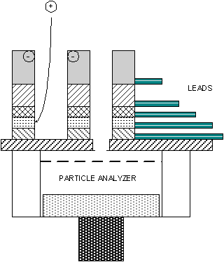
In making
transistors smaller and smaller, one also has to scale the thickness of the
insulating oxi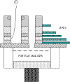 de layer on the "gate" down to less than 50
Angstroms. Etching these oxide layers is problematic, because plasma
processing can cause large voltages to build up across these gates and ruin
their electrical properties. A mechanism called Electron Shading Damage
was postulated some time ago to explain why this happens. Former student
Tsitsi Madziwa devised a program to compute the ion trajectories as they enter a
trench and charge up the sidewalls. She found that there was also ion
shading, and that these trajectories could not cause notches at the trench
bottoms.
de layer on the "gate" down to less than 50
Angstroms. Etching these oxide layers is problematic, because plasma
processing can cause large voltages to build up across these gates and ruin
their electrical properties. A mechanism called Electron Shading Damage
was postulated some time ago to explain why this happens. Former student
Tsitsi Madziwa devised a program to compute the ion trajectories as they enter a
trench and charge up the sidewalls. She found that there was also ion
shading, and that these trajectories could not cause notches at the trench
bottoms.
The DC magnetic field required by
helicon sources is usually produced by large electromagnets driven by powerful
DC power supplies. This cumbersome equipment has been replaced by
our patented invention in which permanent magnets are used in a novel way,
greatly reducing the size, power, and cost of commercial units. More on
this can be found on our laboratory website listed below.
The physics of
partially ionized plasmas has been considered a "dirty science"
because adding neutral atoms to ions and electrons can complicate the problem so
that the solutions are messy. Our aim has been to show that
low-temperature plasma physics need not be low-brow. There are challenging
problems with elegant solutions. As an added bonus, this line of research
has an impact on devices and materials which we use everyday.
For further
information, please visit the website for the LTPTL.