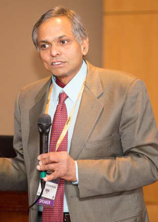
Speaker: Dr. Rama Divakaruni
Affiliation: IBM Distinguished Engineer
Abstract: AI workloads are strongly driving systems to become much more architecturally diverse. Today’s accelerators are composed of a mix of heterogeneous components including CPUs, GPUs, specialized accelerators, and memories. Advanced packaging techniques to enable high inter-connectivity among these components will be crucial for continued progress in AI as this is the key bottleneck for AI Applications. As scaling continues to slow, value at the system level for today’s workloads is achieved more by a diversity of parts, connectivity and bandwidth rather than sheer compute power in a monolithically integrated SoC.
Continued increases in compute performance for modern unstructured data will drive technologies for higher bandwidth including but not limited to 3D stacking. While research has explored advanced cooling techniques — which are viable in a modern data center — a plethora of form factors which will evolve for different AI workloads and is expected to color the landscape. With the advent of analog-based accelerators –also currently in a research phase – it becomes clear to envision a future where a variety of heterogeneously enabled form factors driving different workloads for inference and training are pervasive in the edge and in the Cloud. Thus, AI hardware will be truly packaging to the core!
Biography: Rama Divakaruni received his B.Tech in Electrical Engineering from the Indian Institute of Technology, Madras, India in 1988. He received his Ph.D in Electrical Engineering from the University of California, Los Angeles in 1994. Since 1994, he has been working on advanced semiconductor technologies at IBM. From 1994 through 2003, he worked on DRAM Technology Development and his team introduced the world’s first sub-8F2 vertical transistor DRAM trench technology. From 2004 through 2008 he worked on various strained silicon technologies in both SOI and bulk Si semiconductors. These technologies were the basis of the Nintento Wii, XBOX360 and the PlayStation3 game platforms and at 45nm were introduced into the modern mobile semiconductor fabric. From 2008 through 2013, Dr. Divakaruni worked on IBM’s unique Hi-K technologies and FINFET technologies. Much of this work culminated with the introduction of mobile technologies by IBM’s partners and IBM’s SUMMIT Supercomputer earlier this year using 14nm SOI FINFET technology.
Dr. Divakaruni is currently an IBM Distinguished Engineer and is reponsible for IBM Advanced Process Technology Research. His current focus is on AI Hardware technologies for Deep Learning. He is one of IBMs top inventors with over 225+ issued US patents.
For more information, contact Prof. Subramanian Iyer (s.s.iyer@ucla.edu)
Date/Time:
Date(s) - Oct 12, 2018
10:00 am - 11:00 am
Location:
E-IV Maxwell Room #57-124
420 Westwood Plaza - 5th Flr. , Los Angeles CA 90095
