Speaker: Prof. Yong-Hang Zhang
Affiliation: Arizona State University
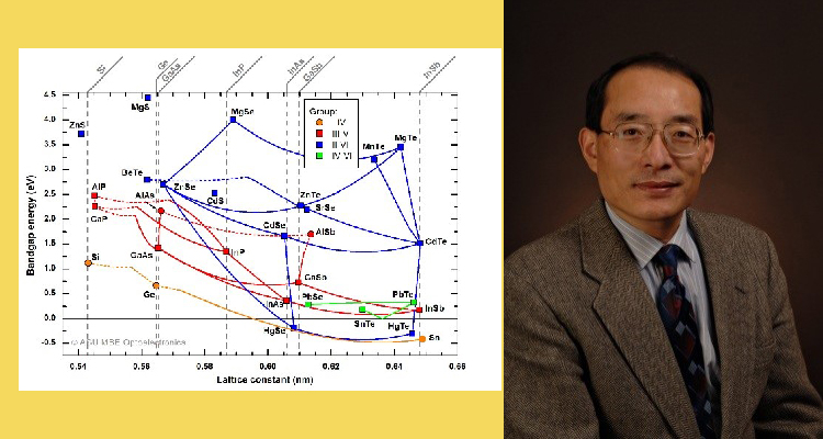
Abstract: Semiconductor electronic and optoelectronic materials and devices have experienced very rapid development for more than half a century. However, there still remains a lack of closely lattice-matched materials and substrates suitable for the monolithic integration of various kinds of semiconductor devices on a single chip. The material platform: II-VI (MgZnCdHg)(SeTe), III-V (AlGaIn)(BiPAsSb), and IV-VI (PbSe, PbTe) semiconductor binaries and their alloys lattice-matched to GaAs, GaSb, InP, InAs and InSb substrates, has been proposed to achieve the goal. These materials have direct bandgaps covering a very broad energy spectrum from far IR to UV (0 ~ 4 eV) and small thermal mismatch. Such a unique material platform not only offers opportunities to study new physics, such as electrical-field-induced topological insulator in heterovalent superlattice and thin-film superconductor on semiconductor (a-Sn/InSb), but also enables new light emitting devices, multi-junction solar cells, multi-color photodetectors, resonant tunneling diodes, and facilitates monolithic integration of various materials without misfit dislocations to ensure the best quality for device applications. This talk will focus on the following topics:
• Latest progress in the MBE growth of these heterovalent structures and their potential applications in the study of interfacial topological insulator states in various heterovalent superlattice like CdTe/InSb, ZnTe/GaSb, and ZnSe/GaAs
• MgxCd1-xTe/MgyCd1-yTe (x=0 and 0.13, y>0.24) heterostructures on InSb substrates with record low interface recombination velocity (~1 cm/s) and ultra-long lifetime (3.6 µs), and crystalline CdTe solar cells with record high efficiency greater than 20%, and 1.7 eV Mg0.13Cd0.77Te solar cell with efficiency of 15% for Si based tandem cell application
• Monolithically integrated CdTe/InSb dual-color photodetectors and midwave IR VCSELs etc.
Biography: Professor Zhang did his research at the Max Planck Institute for Solid States and received this doctoral degree in physics from the University of Stuttgart in 1991. He then worked as an Assistant Research Engineer at UCSB before he joined Hughes Research Labs (HRL) in 1993. In 1996, he was appointed Associate Professor in the Department of Electrical Engineering at ASU and was promoted to full professor in 2000. He edited 3 books, published 3 book chapters and more than 300 peered reviewed papers, presented 400 invited and contributed talks, 14 issued and pending US patents, and advised over 30 PhD students and supervised over 40 postdocs and visiting scholars. He is a fellow of IEEE and OSA, and has served as the Associate Dean for Research at the Fulton Schools of Engineering, director of ASU NanoFab, and is the founding director of the Center for Photonics Innovation, and the Chair of the Governance Board of the University Core User Facility, ASU NanoFab. His areas of research interest include Molecular Beam Epitaxy (MBE) growth of II-VI, III-V, IV-IV, and IV-VI materials, optical properties of semiconductor heterostructures and their applications in solar cells, photodetectors, lasers, transistors. He is currently the chair of both International Conference on MBE and the North America Conference on MBE. More information about his group can be found on the webpage: https://mbe.engineering.asu.edu/.
For more information, contact Prof. Ben Williams (bswilliams@ucla.edu)
Date/Time:
Date(s) - Nov 29, 2018
1:00 pm - 2:00 pm
Location:
EE-IV Shannon Room #54-134
420 Westwood Plaza - 5th Flr., Los Angeles CA 90095