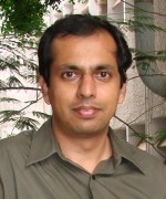
Speaker: Nagendra Krishnapura
Affiliation: Indian Institute of Technology, Madras
Abstract: Delta-Sigma architectures are usually the best choice for high resolution analog-to-digital converters. But when the input is multiplexed from a number of inputs, delta-sigma ADCs cannot be used directly. The memory in the modulator and the decimation filter results in inter-sample interference. To eliminate this, the conversion cycle has to be made long enough for the impulse response of the modulator and decimator to die out before applying the next sample. This results in a substantially lower sampling rate than when the Delta-Sigma ADC is used continuously. Alternatively, the modulator and decimation filter can be reset to realize an incremental delta-sigma modulator. In this case, there is an SNR penalty since the filtering less effective. In this work, it is shown that memoryless analog-to-digital conversion using $\Delta\Sigma$ modulators is possible without resetting the modulator or decimation filters. This is done by constraining the combined signal transfer function for the modulator and a decimation filter to satisfy Nyquist intersymbol interference criterion. This architecture enables memoryless operation over the entire signal bandwidth of the Delta-Sigma modulator which is significantly higher than the bandwidth in incremental architectures in which the modulator is reset. A two-channel ADC with sampling rate of fs/64 per channel is built using a third order 32 times oversampled switched-capacitor modulator. The prototype in 0.18um CMOS occupies 2.1mmsq. At 64MHz sampling rate for the DSM, the standalone modulator consumes 25mW and has a DR/SNRmax/SNDRmax of 85/82/80.3 dB. The sample-and-hold required for multi-channel operation consumes 20 mW. In two-channel mode, with 1 MHz sampling rate per channel, the DR/SNRmax/SNDRmax of 80/76/75 dB. The crosstalk between channels is less than 85 dB. The total power consumption for two channels is 45 mW.
Biography: Nagendra Krishnapura obtained his BTech from the Indian Institute of Technology, Madras, India and his Ph.D. from Columbia University, New York. He has worked as an analog design engineer at Celight, Multilink, and Vitesse semiconductor. He has taught analog circuit design courses at Columbia University as an adjunct faculty. He is currently an Associate Professor at the Indian Institute of Technology, Madras. His interests are analog and RF circuit design and analog signal processing.
For more information, contact Prof. Sudhakar Pamarti (spamarti@ucla.edu)
Date/Time:
Date(s) - Jan 29, 2016
2:00 pm - 3:30 pm
Location:
E-IV Maxwell Room #57-124
420 Westwood Plaza - 5th Flr. , Los Angeles CA 90095
