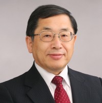
Speaker: Dr. Mitsumasa Koyanagi
Affiliation: GINTI/ Tohoku University, Japan
Abstract: To overcome various concerns caused by scaling-down the device size in future LSIs, it is indispensable to introduce a new concept of heterogeneous 3D integration in which various kinds of device chips with different size, different devices and different materials are vertically stacked. To achieve such heterogeneous 3D integration, a key technology of self-assembly and electrostatic (SAE) bonding has been developed. Exploring new devices for the IoT, we have fabricated several kinds of heterogeneous 3D LSIs called super-chip by stacking compound semiconductor device chip, photonic device chip and spintronic device chip on CMOS device chips using SAE bonding. In addition, we have fabricated 3D stacked CIS (CMOS Image Sensor) chip and 3D stacked multicore processor using reconfigured W2W 3D integration technology with the SAE bonding. These 3D stacked CIS chip and 3D multicore processor are integrated on a Si interposer to achieve the 3D image sensor system module.
Biography: Mitsumasa Koyanagi received the B.S. degree in electrical engineering from Muroran Institute of Technology, Japan in 1969 and the M.S. and Ph.D. degrees in electronic engineering from Tohoku University, Sendai, Japan, in 1971 and 1974, respectively. He joined the Central Research Laboratory, Hitachi Ltd. in 1974 where he worked on research and development of MOS memory device and process technology and invented a stacked capacitor DRAM memory cell which has been widely used in the DRAM production. Stacked capacitor DRAM was the first commercialized 3D LSI. In 1985, he joined the Xerox Palo Alto Research Center, California where he worked on research and development of sub-micron CMOS devices, poly-silicon thin film transistors and the design of analog/digital LSIs. In 1988 he joined the Research Center for Integrated Systems, Hiroshima University, as a professor where he worked on sub-0.1um device fabrication and characterization, device modeling, poly-Si TFT devices, 3-D integration technology, optical interconnection and parallel computer system specific for scientific computation. He fabricated the smallest MOS transistor with a gate length of 70nm at that time which was presented in IEDM 1992. He proposed three-dimensional integration technology based on wafer-to-wafer bonding and Through-Si Via (TSV) for the first time in 1989.
Since 1994, he has been a professor in Intelligent System Design Lab., Department of Machine Intelligent and Systems Engineering (from 1994 to 2003) in Advanced Bio-Nano Devices Lab., Department of Bioengineering and Robotics, Graduate School of Engineering (from 2003 to 2010), and currently New Industry Creation Hatchery Center (NICHe) (from 2010), Tohoku University, Japan where his current interests are 3-D integration technology, optical interconnection, nano-CMOS devices, memory devices, parallel computer system, artificial retina chip and retinal prosthesis chip, brain-machine interface (BMI) and neural prosthesis chip. He established the 3D LSI fabrication facility for 12-inch wafers, GINTI (Global Integration Initiative) in 2013 and became a director. He has been researching three-dimensional integration technology and optical interconnection for more than 20 years. He was a director of the venture business laboratory, Tohoku University from 1998 to 2000 and a Distinguished Professor in Tohoku University from 2008 to 2010. He has published more than 300 technical papers and given more than 100 invited talks.
For more information, contact Prof. Subramanian Iyer (s.s.iyer@ucla.edu)
Date/Time:
Date(s) - Dec 14, 2015
10:30 am - 11:30 am
Location:
E-IV Maxwell Room #57-124
420 Westwood Plaza - 5th Flr. , Los Angeles CA 90095
