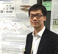
Speaker: Hyunseok Kim
Affiliation: Ph.D. Candidate - UCLA
Abstract: Chip-scale integrated light sources are a crucial component in a broad range of photonics applications. III-V semiconductor nanowire emitters have gained attention as a fascinating approach due to their superior material properties, extremely compact size, and capability to grow directly on lattice-mismatched substrates including silicon. However, their practical applications are still in the early stages due to the difficulties in achieving high-performance nanowire emitters and integrating nanowire emitters with photonic platforms.
Here, we demonstrate III-V nanowire-based lasers monolithically integrated on silicon-on-insulator (SOI) platforms, which can be potentially employed for chip-scale optical communications and photonic integrated circuits. For this, selective-area epitaxy of nanowires on 3D structured SOI platforms is developed by catalyst-free metal-organic chemical vapor deposition. Bottom-up photonic crystal cavities are integrated on the SOI platforms using this method, wherein InGaAs/InGaP core/shell nanowire arrays form 1D and 2D photonic crystals. Single-mode lasing is achieved from these cavities by optical pumping, and these nanowire array lasers are effectively coupled to SOI waveguides. The lasing wavelengths of nanowire array lasers are in the ranges of 1,100–1,440 nm, which covers telecommunication wavelengths, all operating at room temperature. It is also shown that arrays of nanowire lasers with individually tunable wavelengths can be integrated on a single chip by lithographically tuning the cavity geometries. In summary, the III-V nanowire lasers on silicon demonstrated here represent a new platform for ultracompact and energy-efficient light sources for silicon photonics and unambiguously point the way toward practical and functional nanowire lasers.
Biography: Hyunseok Kim is currently a Ph.D. candidate in the Department of Electrical and Computer Engineering under the supervision of Prof. Diana L. Huffaker. His interest is on nanowire-based nanophotonics, optoelectronics, and quantum optics. He received his B.S. and M.S. in Electrical Engineering in 2011 and 2013, respectively, from Seoul National University in South Korea. Before joining UCLA, he was a junior researcher at Korea Institute of Industrial Technology in South Korea.
For more information, contact Prof. Diana L. Huffaker (huffaker@ee.ucla.edu)
Date/Time:
Date(s) - Aug 02, 2018
1:00 pm - 2:30 pm
Location:
E-IV Tesla Room #53-125
420 Westwood Plaza - 5th Flr., Los Angeles CA 90095
