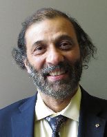
| Research and Teaching Interests:
System Scaling Technology, advanced packaging and 3D integration, technologies and techniques for the memory subsystem integration and neuromorphic computing |
||
| Awards and Recognitions |
| 2020 | IMAPS Daniel C. Hughes, Jr. Memorial Award |
| 2017 | National Academy of Inventors (NAI) Fellow |
| 2016 | American Physical Society (APS) Fellow |
| 2012 | IEEE Daniel Noble award for Emerging Technologies |
| 2011 | Asian-American Engineer of the Year (awarded by the Society of Chinese Engineers in 2011) |
| 2010 | IBM Fellow |
| 2009 | IBM Master Inventor |
| 2004 | Distinguished Alumnus of the Indian Institute of Technology, Bombay |
| 2002 | IBM Distinguished Engineer |
| Two IBM Corporate awards for the development of embedded DRAM and electrical Fuses | |
| Four IBM Outstanding Technical Achievement awards for development of the first SiGe base HBT, “Salicide”, eDRAM and eFUSES | |
| 30 Invention Plateaus at IBM. | |
| 1995 | IEEE Fellow |
| Selected Publications |
- Iyer, S.S. “Three-dimensional integration: An industry perspective” (2015) MRS Bulletin 40 (3) pp225-232 (2015)
- S Rosenblatt, D Fainstein, A Cestero, J Safran, N. Robson,T. Kirihata and S.S. Iyer, (2013) “Field tolerant dynamic intrinsic chip ID using 32 nm high-K/metal gate SOI embedded DRAM” IEEE JSSCC 48(4) pp940-947.
- S.S. Iyer, “The evolution of dense embedded memory in high performance logic technologies”, (2012) IEDM Proceedings pp 33.1.1-33.1.4
- Farooq, M. G., & Iyer, S. S. (2011), “3D integration review”. Science in China 54(5), 1012-1025 (2011)
- Iyer, S. S., Freeman, G., Brodsky, C., Chou, A. I., Corliss, D., Jain, S. H., … & Agnello, P. (2011). 45-nm silicon-on-insulator CMOS technology integrating embedded DRAM for high-performance server and ASIC applications. IBM Journal of Research and Development, 55(3), 5-1.
- Barth, J., Reohr, W. R., Parries, P., Fredeman, G., Golz, J., Schuster, S. E., … & Iyer, S. S. (2008). A 500 MHz random cycle, 1.5 ns latency, SOI embedded DRAM macro featuring a three-transistor micro sense amplifier. Solid-State Circuits, IEEE Journal of, 43(1), 86-95.
- Kirihata, T., Parries, P., Hanson, D. R., Kim, H., Golz, J., Fredeman, G., … & Iyer, S. S. (2005). An 800-MHz embedded DRAM with a concurrent refresh mode. Solid-State Circuits, IEEE Journal of, 40(6), 1377-1387
- Kothandaraman, C., Iyer, S. K., & Iyer, S. S. (2002). Electrically programmable fuse (eFUSE) using electromigration in silicides. Electron Device Letters, IEEE, 23(9), 523-525
- Powell, A. R., & Iyer, S. S. (1994). Silicon-Germanium-Carbon Alloys Extending Si Based Heterostructure Engineering. Japanese journal of applied physics, 33(part 1), 2388-2391.
- Iyer, S. S., & Xie, Y. H. (1993). Light emission from silicon. Science, 260(5104), 40-46.
- Gennser, U., Kesan, V. P., Iyer, S. S., Bucelot, T. J., & Yang, E. S. (1990). Resonant tunneling of holes through silicon barriers. Journal of Vacuum Science & Technology B: Microelectronics and Nanometer Structures, 8(2), 210-213.
- Iyer, S. S., Patton, G. L., Stork, J. M., Meyerson, B. S., & Harame, D. L. (1989). Heterojunction bipolar transistors using Si-Ge alloys. Electron Devices, IEEE Transactions on, 36(10), 2043-2064.
- Iyer, S. S., Metzger, R. A., & Allen, F. G. (1981). Sharp profiles with high and low doping levels in silicon grown by molecular beam epitaxy. Journal of Applied Physics, 52(9), 5608-5613.
